NVMe™ Form Factors Blog Series Part II: “NVMe Building Blocks – Controller, Buffer Memory, Media and Form Factors”
BlogBy J Metz and Bill Lynn
Thank you for joining us for Part II of our blog series, “NVMe Form Factors”. If you missed part I, you can catch up here. Now let’s get down to the topic at hand—the building blocks of NVMe™.
Building Blocks
An SSD consists of an SSD controller chip, some DRAM buffer memory, and the storage media (in this case NAND flash chips) assembled on a printed circuit board (PCB). The physical dimensions of the SSD is what is known as the form factor. The figure below is a simple block diagram of a typical SSD.
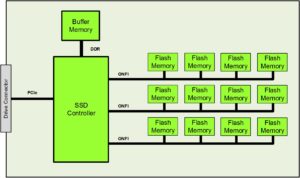
Controller
The SSD controller chip is the heart of the SSD and bridges the gap between the host interface and the physical storage media.
The controller chip translates incoming commands from the host into the necessary actions needed to either read or write/program the physical storage media. For a typical SSD the controller chip determines the placement of the data among the flash chips and maintains a data placement table in its Flash Translation Layer (FTL).
Additionally, the controller chip also does all of the housekeeping tasks – like making sure unused flash has been erased – and is ready to be programmed (a process known as garbage collection) and evenly distributing writes among the various flash chips (also known as wear leveling).
Buffer Memory
The buffer memory is used as a cache to hold incoming data in preparation for writing to the flash chips since the process of programming a flash chip is relatively slow.
Different kinds of SSDs handle buffer memory in different ways. In high performance SSDs, for example, this is a separate DRAM chip. However, in lower-end SSDs a smaller buffer memory may be integrated into the controller chip. Very low-end client SSDs may not have any resident buffer memory at all, using a part of the host memory instead.
Cache memory has the potential to greatly improve the write performance of the SSD, but care must be taken to protect any data in the memory in the event of an unexpected power loss. This feature is known as PLP or Power Loss Protection. The existence (or non-existence) and location of where this memory is placed can make a big impact on the form factor of the device.
Media
Media refers to the physical devices that are used to store user data. (Quick note: media is the correct plural term for medium; “mediums” don’t exist in data centers, unless of course you’re holding a séance among your servers!)
For typical SSDs the media is a collection of NAND flash chips. However, media evolves over time, and so NVMe was architected to abstract the media characteristics so that SSDs could be built with different types of non-volatile memory. Technologies such as phase change memory (PCM) or magnetoresistive random-access memory (MRAM) are potential candidates for newer SSD media. As non-volatile memory evolves, NVMe based SSDs should be able to take advantage of improved density, performance, and endurance.
Typically the performance characteristics of non-volatile memories tend to be slower than the performance capabilities of the host interface. The goal of most SSD architectures is to balance the performance of the front-end host interface with the performance capabilities of the back-end storage media. To achieve this balance most SSD controller chips may have multiple back-end storage interfaces or channels. For NAND flash SSDs these would be ONFI flash channels.
Form Factor (or, How We Learned To Love Alphabet Soup)
The form factor defines the physical dimensions and connectors used by an SSD. A specific SSD form factor may support multiple host interfaces. There are many different form factors currently defined by multiple standards bodies that could be used to implement an SSD. For example there are the following:
- Drive form factors (2.5” and 3.5” connected by SAS and SATA) defined by SFF-8301 [SFF-8301 & SFF-8201] & SFF-8201.
- U.2 drives (2.5” drive connected by SAS, SATA, or PCIe) defined by SFF-TA-1000, is a PCIe x4 SSD in the 2.5in x 15mm or 2.5in x 7mm form factor.
- A U.2 connector (formerly known as SFF-8639) supports multiple host interfaces, for instance,
- PCIe, SAS, and SATA.
- PCIe adapter cards (Full-Height/Full Length (“FH/FL”), Half-Height/Half-Length (“HH/HL”) connected by PCIe) defined by PCI-SIG.
- M.2 modules (22x30mm, 22x42mm, 22x80mm, and 22x110mm connected by SATA and PCIe) defined by PCI-SIG (there is a good overview by SNIA on M.2 here).
- EDSFF form factors (connected by PCIe) defined by SFF-TA-1006, SFF-TA-1007, and SFF-TA-1008.
- Single chip Ball Grid Array (“BGAs”) (16mm x 20mm and 11.5mm x 13 mm connected by PCIe) defined by PCI-SIG.
- SD-PCIe cards (connected by PCIe) defined by SDA (More info here).
CF Express cards (connected by PCIe) defined by CFA.
For more information on SSD form factors, visit the SNIA website.
Breaking Things Apart To Put Them Back Together Again
Taking a look at the building blocks above can make it easier to see how they interrelate – regardless of what the final device looks like. When we look at how they do interrelate, though, we start to see how these trade-offs occur.’
For example, there are a number of factors that affect, say, capacity:
- Number of back end channels supported by the controller
- Number of flash placements on the SSD (or physical size of the SSD form factor)
- Capacity of individual flash chips
- The amount of over provisioning implemented
The total raw capacity of the SSD is equal to the number of flash chips times the capacity of each chip. The number of flash chips that can be supported on an SSD is determined by the SSD form factor (physical size) and the number of chips that can be connected to the SSD controller chip.
3D NAND technology increases the capacity of the individual flash chips by stacking NAND layers vertically within a chip. This technology greatly increases the capacity but does nothing to increase the performance.
Another factor that affects capacity of an SSD is the amount of what’s called over-provisioning. Flash chips can only go through a limited number of program- and erase-cycles before they fail. This is known as endurance and is measure by “drive-writes-per-day” (DWPD) or” total terabytes written” (TBW). SSDs will take, or over-provision, some percentage of their raw capacity and set it aside to replace failed NAND cells over the lifetime of the SSD to increase their overall reliability. This percentage can be as high as 50% for high endurance SSDs.
Looking at what affects the capacity of an SSD is relatively straightforward. Looking at what affects the performance of an SSD, however, is much more complex. For one thing, performance includes bandwidth and latency. For NAND flash-based SSDs we also have the issue of read/write asymmetry; meaning, reads are much, much faster than writes.
Factors that affect the overall performance of an SSD include:
- Form factor and host interface of the SSD
- Number and performance of the back-end device interfaces
- Number and performance of the actual storage devices
- Amount of power allocated for the SSD
- Efficiency of the storage protocol
- Efficiency of the host storage driver
With SSDs the host interface dictates the maximum potential performance. Performance of current SSD host interfaces include the following:
- 6Gb/s SATA approximately 540MB/sec
- PCIe Gen 3 x1 approximately 800MB/sec
- 12Gb/s SAS (SAS 3) approximately 1.2GB/sec
- PCIe Gen 3 x4 approximately 3.2GB/sec
- PCIe Gen 3 x8 approximately 6.4GB/sec
- PCIe Gen 3 x16 approximately 12.8GB/sec
Now that we’ve analyzed the different building blocks for NVMe, we’ll bring it all together next time in part III, “The Importance of Form”, the final installment of our “NVMe Form Factors” blog series.